Hpack – MMIC Package
To reduce the burden of your engineering resources on pack-aging, and shorten your “Time to Market”
- Open-tooled Air-Cavity QFNs, common body size and lead counts available
- Custom design on Air-Cavity / Overmold QFN provided
- High familiarity of handling Gas/GaN MMICs, and high power materials such as sintered Ag. high thermal conductivity substrates
- Proper solution for both rapid prototyping and high volume production
- Reasonable Leadtime and NRE cost
Final Package Test
WHY WE DO THE FINAL PACKAGE TEST
Final package test is an essential step in the semiconductor industry to ensure that the casing (package) of a semiconductor device meets the quality standards and specifications after the process is completed.
When semiconductors are manufactured, dies (process-finished wafers) need to be packaged in protective enclosures to protect them from damage and provide connectors to connect to electronic systems.
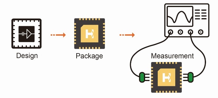
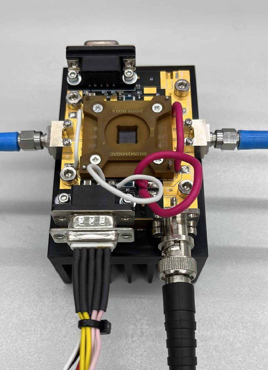
Final package test ensures that packaged semiconductor devices can operate normally and maintain stable performance under various conditions. Our Final package test can obtain the package’s electrical characteristics (such as S-parameters, output power, power efficiency, noise figure, and so on)


